Samsung Unveils Next-Gen 3D Memory Tech: Industry's First zHBM Concept and 400+ Layer V10 NAND Make a Grand Debut
2026-08-12

Samsung Electronics has announced its latest AI memory product portfolio and technology roadmap at FMS (Future of Memory and Storage). The tech giant showcased the industry's first zHBM and zNAND-O concept products, the V10 BV-NAND featuring over 400 layers, and a comprehensive suite of solutions aimed at advancing the infrastructure of future AI.
zHBM and zNAND-O: Defining the Outer Limits of Next-Gen 3D Memory
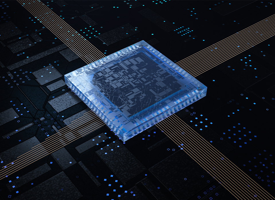
Making its global debut, Samsung's zHBM concept model disrupts traditional design—which places the HBM and AI processor side by side—by vertically stacking the HBM directly on top of the accelerator. This drastically shortens data transmission distance. Purpose-built for advanced AI computing, zHBM delivers much higher bandwidth and power efficiency. According to Samsung:
Performance: Next-gen interface systems adopting zHBM are expected to deliver approximately 8 times the performance of HBM5.
Density & Efficiency: Paired with next-gen wafer bonding technology, zHBM's storage density can reach over 10 times that of HBM5, while improving energy efficiency by 3x and cutting thermal resistance by more than half.
Customization: zHBM supports fully customized designs, allowing clients to integrate proprietary IP into the interposer between the storage and the accelerator, further expanding capacity and performance.
Samsung also introduced zNAND-O, a next-generation high-performance NAND solution based on its V-NAND technology, currently under development in 4-layer and 8-layer versions. Offering high space utilization, optimized I/O performance, and low latency, zNAND-O is tailor-made for edge AI environments supporting real-time, data-intensive AI applications.
V10 BV-NAND: A New NAND Milestone 13 Years in the Making
It has been 13 years since Samsung first introduced its V-NAND technology at FMS 2013. At this year's event, Samsung took off the wraps of its V10 BV-NAND flash memory, which adopts a brand-new Bonded V-NAND (BV-NAND) architecture.
Boasting over 400 layers, the product achieves storage cell stacking through wafer bonding technology.
Its bit density sees an approximate 58% leap compared to the previous generation, V9.
It delivers generational breakthroughs in read, write, and I/O performance, providing high-performance, ultra-large-capacity NAND support for future AI systems and demanding workloads.
Complete AI Memory Roadmap Revealed: From HBM to PIM and Enterprise Storage
Samsung simultaneously displayed its latest AI memory and storage portfolio—including HBM4E, HBM5, LPDDR5X-PIM, and PM1763—highlighting its technological roadmap for next-gen AI computing and data center infrastructure.
Following its industry-first mass production of HBM4 using 1c DRAM and a 4nm base die technology in February this year, Samsung began delivering HBM4E samples to global customers in May, cementing its leading position in the HBM sector.
Additionally, the LPDDR5X-PIM showcased at the event is the industry's first LPDDR memory integrated with Processing-in-Memory (PIM) technology. This solution processes data directly inside the memory, drastically enhancing data transfer efficiency and curbing power consumption.
On the enterprise storage front, new powerhouses like the PM1763 and BM1773 were also on display, aimed squarely at the skyrocketing storage demands of AI data centers.